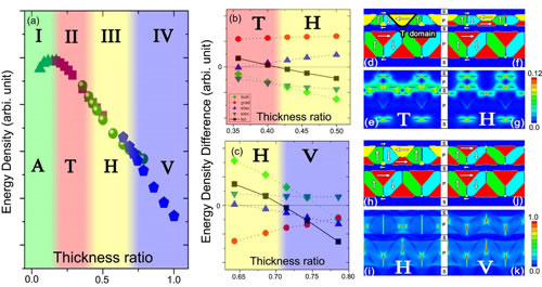
Figure 1. Aberration-corrected transmission electron microscopy analysis of a PTO/STO multilayer film with a thickness ratio of 1 between adjacent PTO layers. A periodic V-domain array appears in each PTO layer and also exhibits periodicity in the vertical film direction. (ac) Low-power TEM brightfield image (a), electron diffraction spectrum (b), and high-power HAADF-STEM image (c) of the PTO/STO multilayer film; (df) geometric-phase analysis of graph (c) The obtained in-plane lattice strain (d), out-of-plane lattice strain (e) and in-plane lattice rotation (f) two-dimensional distribution map. Figure 2. Aberration-corrected transmission electron microscopy analysis of a PTO/STO multilayer film with a thickness ratio of 0.5 for adjacent PTO layers. The periodic V domain array appears in the thicker PTO layer, while the regularly arranged H domain array appears in the thinner PTO layer. (a) TEM bright field image of a PTO/STO multilayer film. (b) HAADF-STEM image of the film. (c, d) Two-dimensional distribution of in-plane and out-of-plane lattice strains obtained from the geometric phase analysis of (b). (e,f) Two-dimensional maps of out-of-plane and in-plane lattice rotations corresponding to (b). (g,h) A magnified HAADF-STEM image of a thin PTO layer. Figure 3. The superposition of polarization vector and the original image clearly shows the flux fully closed ferroelectric domains with symmetry characteristics. Figure 4. Schematic (ab) and dislocation strain analysis (cf) for arrays of V and H domains. (c) Schematic diagram of lattice strains in vertical and (d) horizontal fully closed domain structures. (e) When the adjacent PTO layers have the same thickness, the periodic vertical full closure facilitates the accommodation of the strain. (f) When the thickness ratio of adjacent PTO layers is 1/2, horizontal full closure in the thin PTO layer facilitates the strain contained therein. Figure 5. Phase field simulation of a multilayer PTO/STO thin film system. (a) A phase diagram of the domain structure in the PTO as a function of the thickness ratio in the adjacent PTO layers. There are four domain regions I, II, III, IV corresponding to a1/a2 domain (A), trapezoidal a domain (T), horizontal fully-closed domain structure (H) and vertical fully-closed domain structure (V). (b) Difference in energy density between the H domain and the T domain near the second transition point. (c) Difference in energy density between the V domain and the H domain near the third transition point. Domain configurations and elastic energy density distribution diagrams for T domains (d, e) and H domains (f, g). Domain configurations and elastic energy density distribution maps of H-domain (h, i) and V-domain (j, k). Institute of Metal Research, Chinese Academy of Sciences Shenyang Institute of Materials Science, National Solidarity Research Institute Ma Xiuliang, Zhu Yinlian, and others collaborated with American scientists to make new progress in the periodic array of ferroelectric domains with fully closed fluxes and their controlled growth. A phase diagram of a two-dimensional periodic array of flux-closed ferroelectric domains was established and a clear atomic structure map was obtained. Topological defects have unique characteristics of force, electricity and magnetism, and have important application value in electronic devices. As an important topological defect, ferroelectric vortex domains with closed-polarization distribution or flux-enclosed domain configurations have a wide application prospect in high-density data storage. Since the use of a fully enclosed domain structure to store data can avoid the mutual influence between data, if such a nano-domain configuration can be prepared into a periodic array, it will facilitate the data addressing. Shenyang Materials Science National (Joint) Laboratory Solid Atomic Imaging Department Material Interface Electron Microscopy Research Team Collaborated with Shenzhen Institute of Advanced Technology, Chinese Academy of Sciences, Professor Li Jiangyu of the University of Washington, USA, and Dr. Li Zhihao of St. Louis University, USA, to use aberrations to correct transmission. Electron microscopy combined with phase field simulation techniques has made progress in the study of two-dimensional periodic closed domains. Based on the one-dimensional periodic full-closed domain configuration discovered by the research team in the previous stage, by controlling three-dimensional strain states, a two-dimensionally ordered array of flux fully-closed arrays can be controllably prepared and can be predicted by phase field simulation. Two-dimensionally ordered fully-closed arrays have conditional phase diagrams. The research results were published online on November 16 in the Nano Express. Strain has a major influence on the functional properties and microstructure of functional oxides, especially on ferroelectric materials. In the previous work, the research team found a one-dimensional periodic arrangement in the PbTiO3/SrTiO3 (PTO/STO) thin film system by adjusting the two-dimensional strain state (using a GdScO3 substrate that provides tensile strain in two directions in the plane). An array of vertical fully-closed domains (V-domains) of 180° domain walls along the vertical interface direction. This domain configuration has asymmetrical properties in the spatial configuration. Based on this, the researchers designed and prepared a thickness-modulated PTO/STO multilayer film based on the huge dislocation strain characteristics of fully closed domains in the tetragonal ferroelectrics. The multilayer film is in-plane strain-modulated by the substrate, and the out-of-plane strain is also effectively regulated, that is, the entire film is in a three-dimensional strain state. Aberration-corrected transmission electron microscopy analysis shows that when the thickness of adjacent PTO layers is the same, the fully-closed domains (V domains) of the 180° domain wall in the vertical direction are periodically arranged in-plane and show periodical out-of-plane as well. When the thickness ratio of the adjacent PTO layer is 0.5, a periodic V-domain array still appears in the thick PTO layer, while a regular arrangement occurs in the thin PTO layer. The domain structure (H-domain) of the 180° domain wall is fully closed in the horizontal direction, and a regular fully-closed domain array in which H domains and V domains are alternately arranged is obtained. Based on the aberration-corrected electron microscopy analysis, the researchers simulated the phase field by changing the thickness ratio of adjacent PTO layers. From the perspective of the competition between elastic energy, electrostatic energy, and gradient energy, the researchers established The phase diagram of the evolution of the domain structure of the system with thickness ratio. Based on the results of the phase field simulation, the verification of a large amount of experimental data in this work was carried out. The research results further improve the importance and effectiveness of strain-controlling the domain structure and physical properties of ferroelectric materials, and provide a new approach for exploring high-density information storage based on ferroelectric materials. It is important for the design and development of new nano-devices. significance. The research work was supported by the National Natural Science Foundation of China, the Frontier Science Key Research Project of the Chinese Academy of Sciences, and the National Basic Research Development Program (973 Program). There are two main Bonded NdFeB Magnet manufacturing methods: Bonded Compression Moulding NdFeB Bonded Compression Moulding Ndfeb,Ndfeb Arc Bonded Magnet,Ndfeb Block Bonded Magnet Jinyu Magnet (Ningbo) Co., Ltd. , https://www.magnetbonwin.com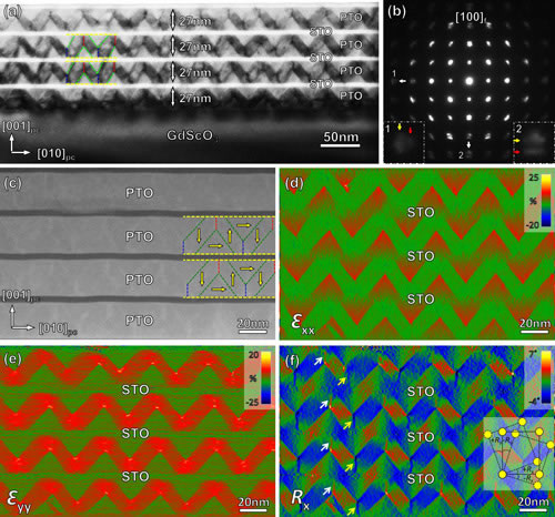


ï‚·Bonded Injection Plastic Moulding NdFeB
ï‚·Bonded Compression Moulding Ndfeb
Bonded Compression Moulding NeFeB Magnets ( called Compression Bonded Magnets) are made by using many isotropic Neodymium, Iron, Boron materials, as well as crushed and powdered Samarium and Cobalt ingredients.Combinations of different elemetal grades are used to creat specific magnetic properties. Compression Bonded Magnets offer higher magnetic strength than Injection Plastic moulded magnets. Although Compression Bonded Magnets have higher magnetic particle density, ther are limeted to simple geometric shapes due to the compaction process. The epoxy is used to protect the magnet surface from industrial solvent and automotive fluids. The normal applications of the magnets range from -40℃ to 150℃.
The advantages of Compression Bonded Magnets:
1. High quantity and even volume manufaturing, with up to millions of pieces per year
2. Single-time moulding and multi-poles orientation.
3. Effective surface treatment to prevent corrosion. The product is coated with epoxy resin to be protect the surface smoothing.
4. Excellent magnetic properties. The energy of Compression Bonded Magnets is 3 times as high as anisotropic ferrite magnets.
Application of Compression Bonded magnets:
•Mini motors
•Automatic contolling devices
•Sensors
•Drivers
•Telecom